During the Thanksgiving break the family thoughts turned to Christmas gifts. My son expressed an interest in a programmable robot so I
started searching for suitable products to satisfy that desire, coming across the Arduino system in the process. After some discussion we
decided not to go in that direction for my sons Christmas gift but having researched the platform a little and downloaded the software to
try it out I had an idea that maybe there were some moderately straight forward projects that could be achieved with the platform.
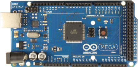
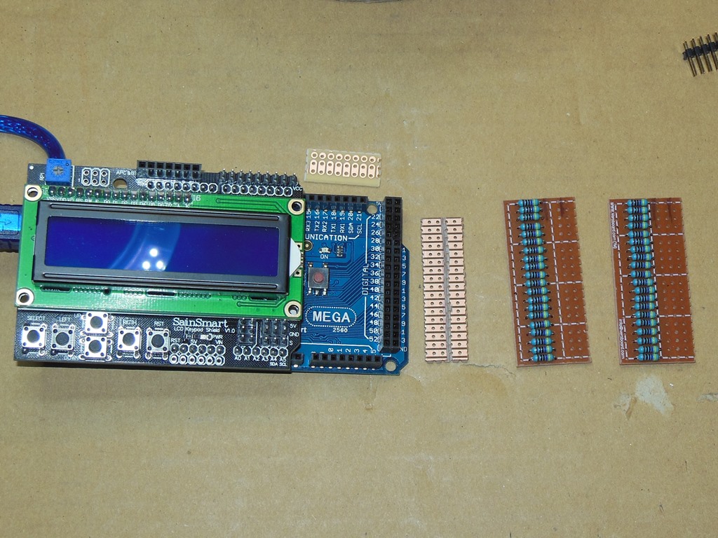
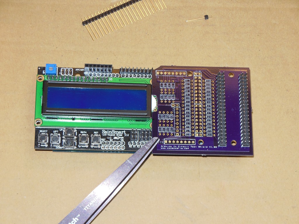
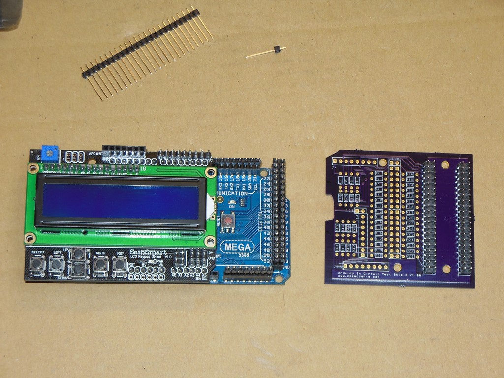
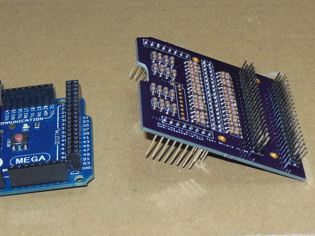
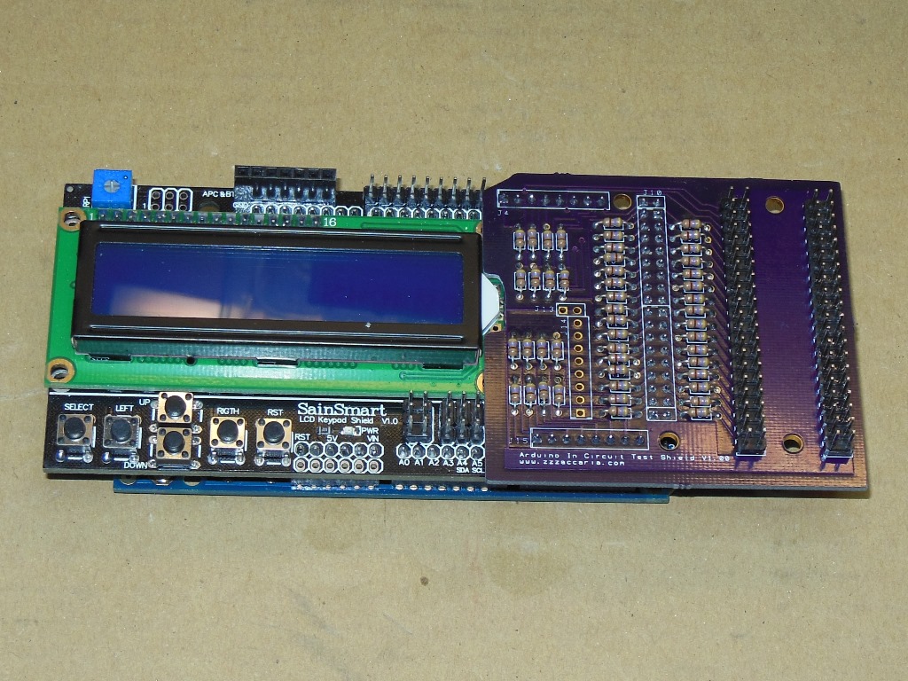
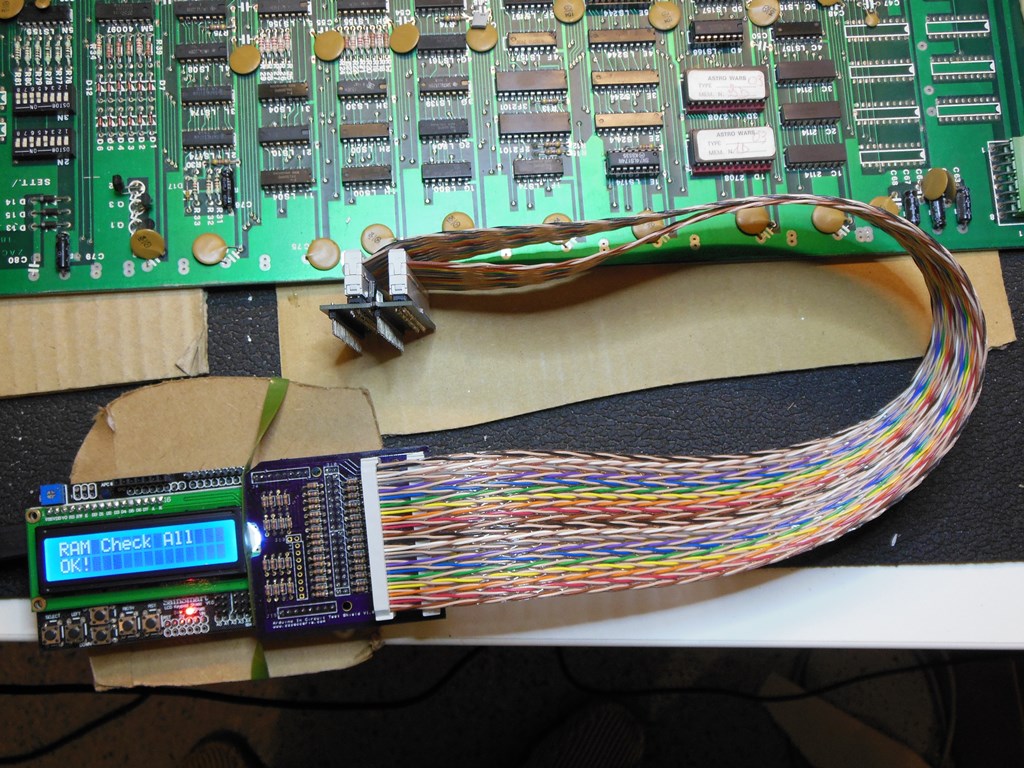
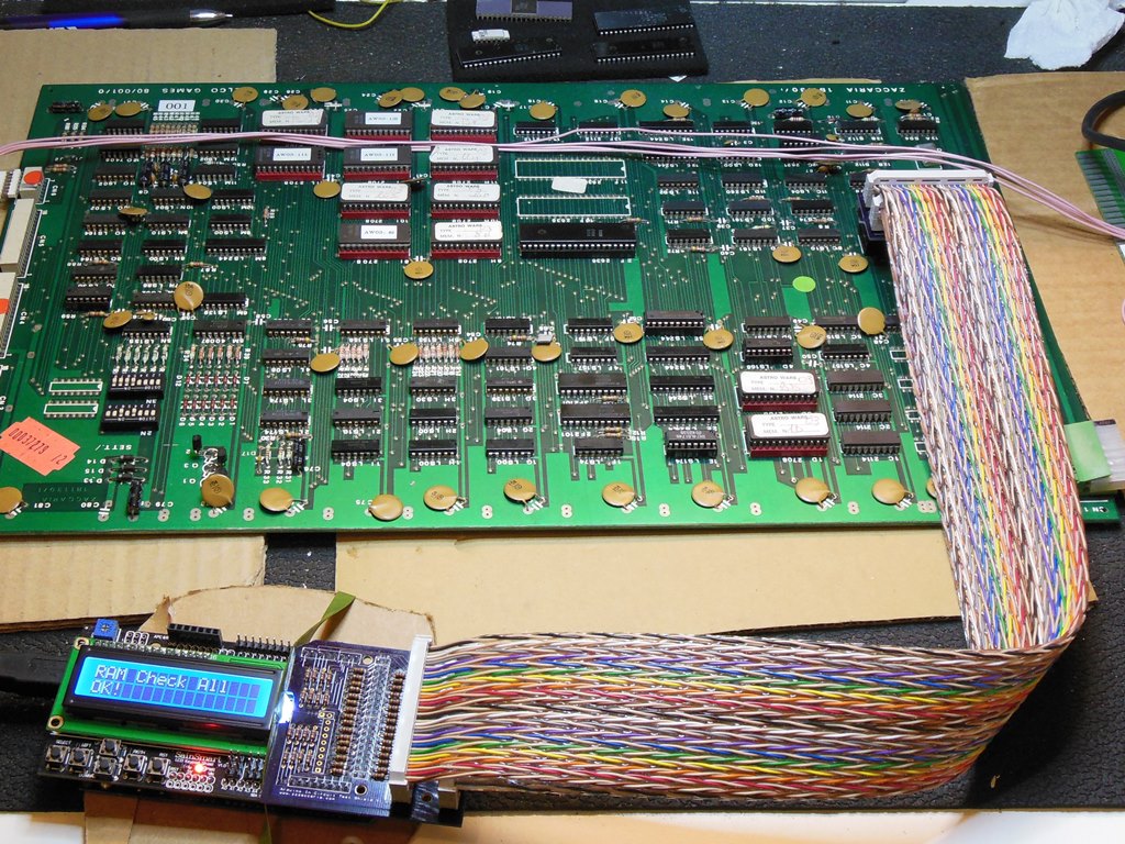
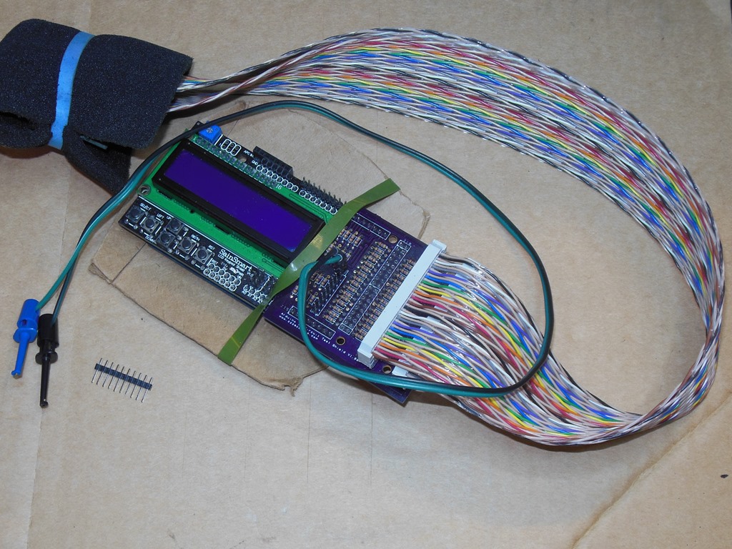
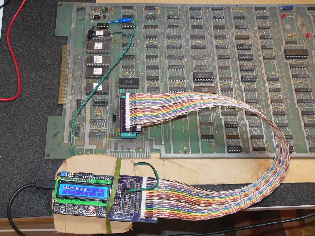
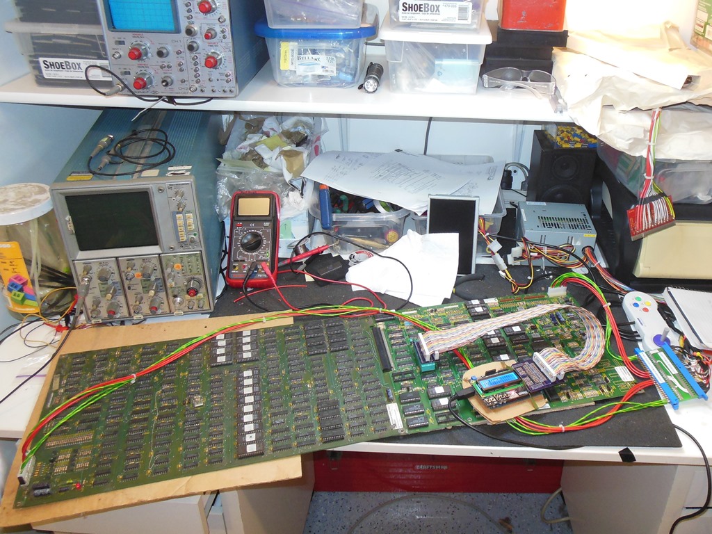
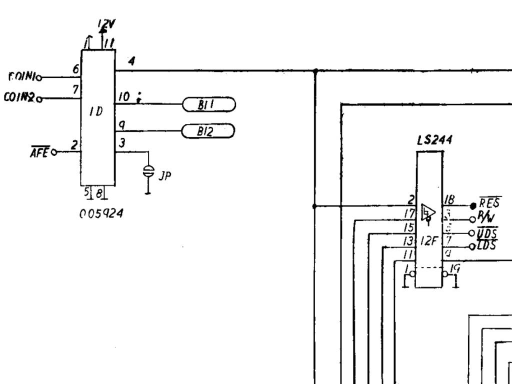
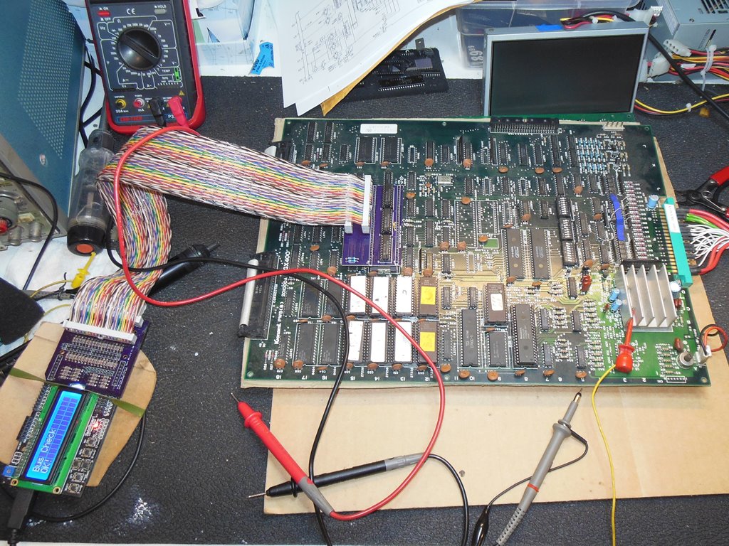
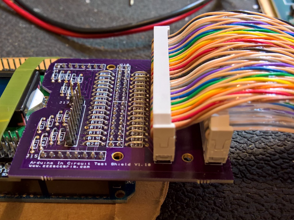
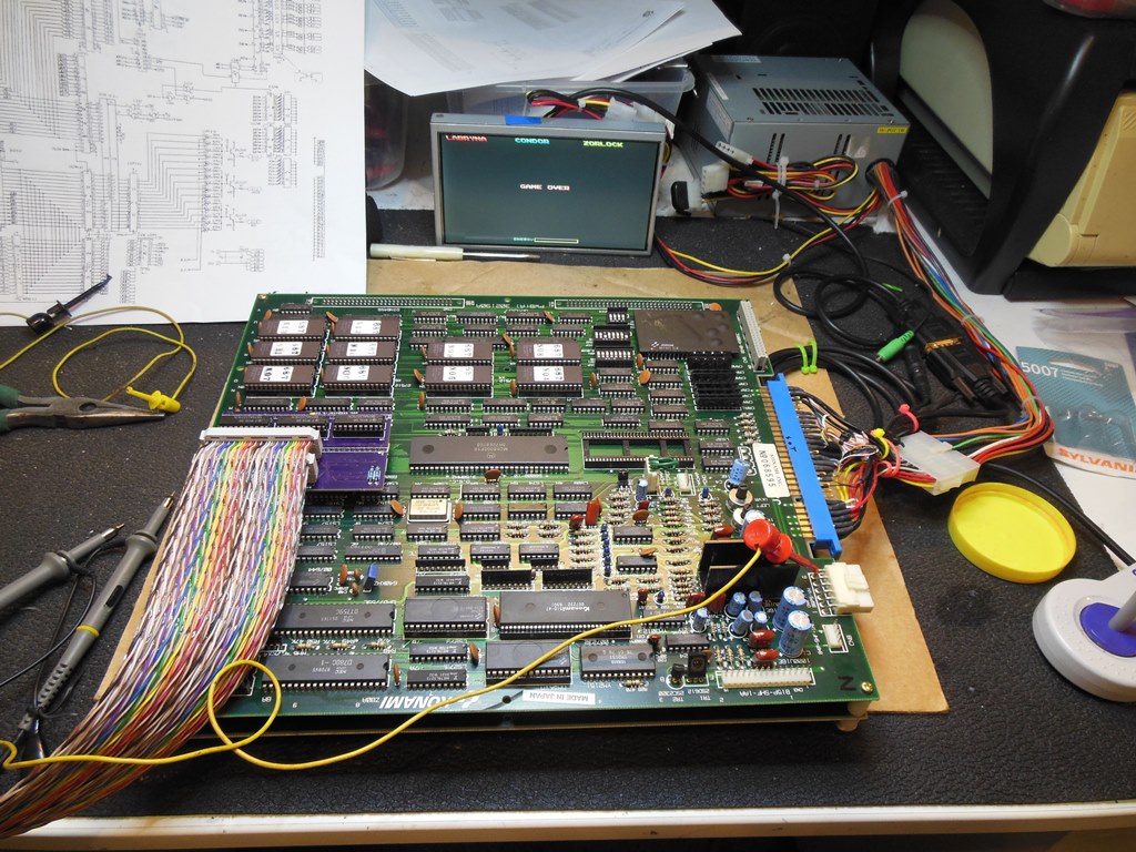
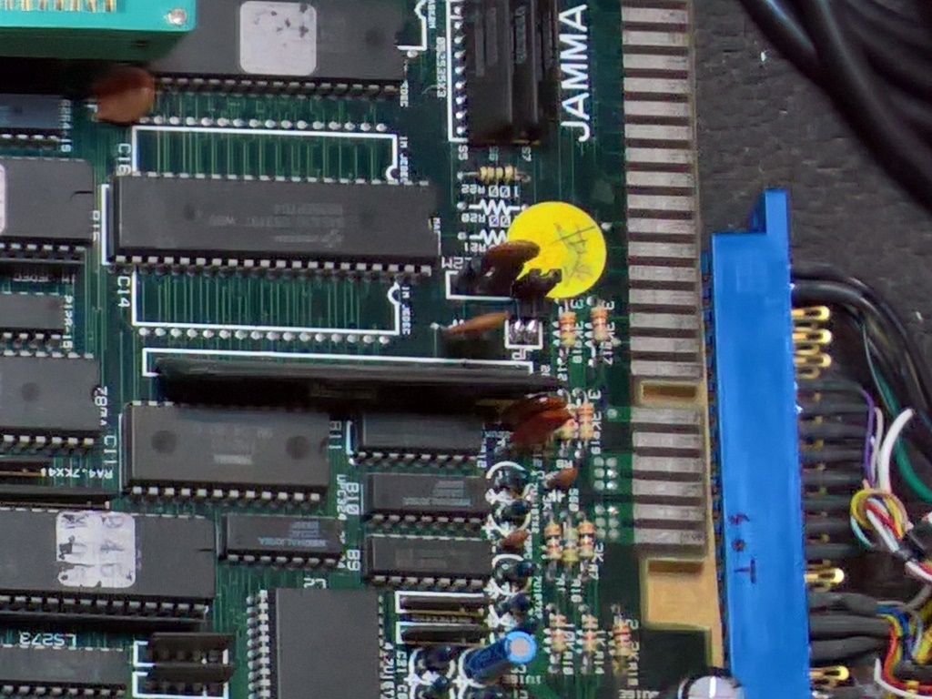
One piece of equipment I'm in need of is a way to test Zaccaria 2650 processor based games (The Invaders, Astro Wars, Quasar, Lazarian etc.). There is no native Fluke 9010 series pod for this processor though there is a published circuit to adapt a Z80 pod for use in 2650 circuits (though no Run UUT of course). Previously I'd thought that at one point I'd design and build myself a native 2650 pod out of parts from rarely used pods. Now I've found the Arduino Mega platform that has 54 digital IO lines (enough to drive a 40-pin DIL package) and is based on C programming (that's my day job) I wondered if this might make the basis of a very simple software programmable in- circuit tester. It would be very simple hardware wise - an Arduino Mega 2560, LCD/input shield and a small kludge to connect 40 of the digital IO lines to a Fluke 40-pin UUT cable assembly recovered from a rarely used pod. The rest would be all software to drive the pins the right way.
Since all the 2650 platforms are all similar Zaccaria implementations the requirement is only that the tester is compatible with these
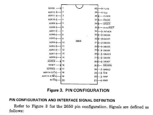
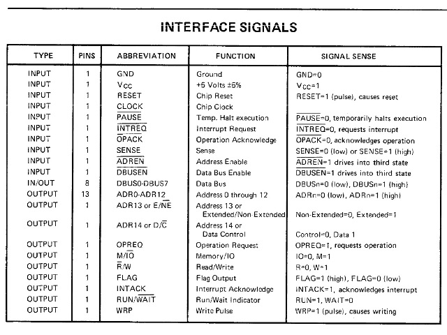
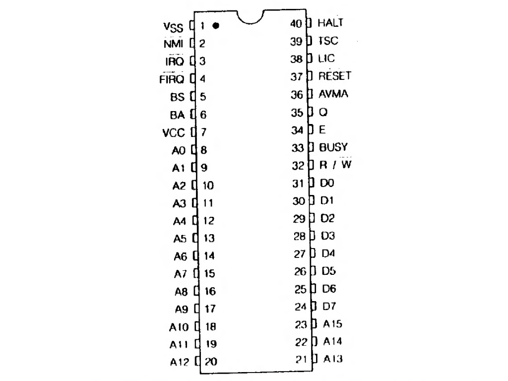
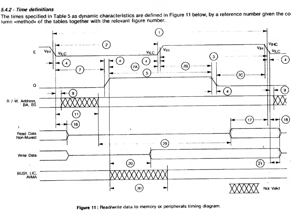
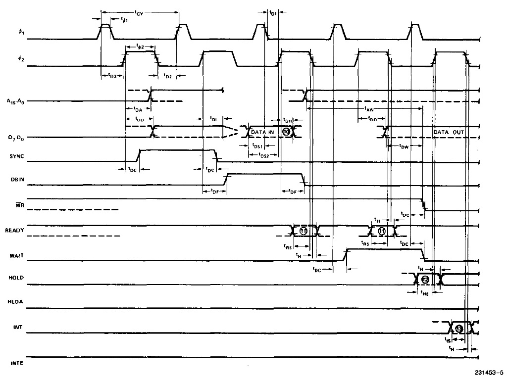
particular platforms. The first thing to check is what the 2650 bus cycles look like. These are the relevant diagrams from the 2650
manual:


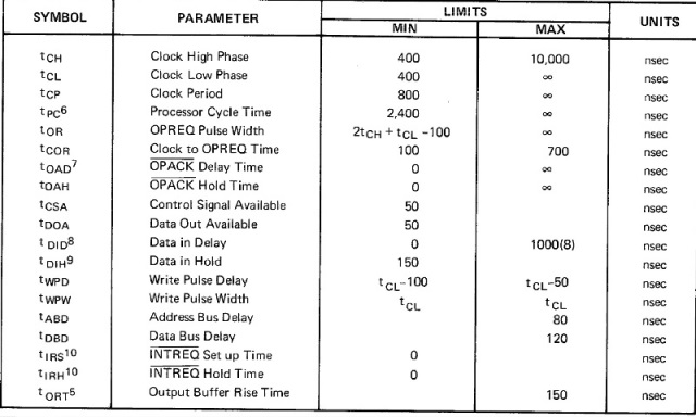
In general it looks straight forward - on a write the 2650 drives address, data and control onto the bus then asserts OPREQ. That state
remains until the memory responds by asserting ~OPACK to terminate the cycle. Similarly on a read, the 2650 drives address and control
onto the bus and then asserts OPREQ. It then clocks in the read data when the memory responds by asserting ~OPACK. In the write cycle the
2650 also asserts a ~WP as a 300ns "write pulse" to clock data into the external memory.
Any circuit that has an exact dependence on the exact timing of the signals against the CPU clock won't work properly with simple pin IO. Possible trouble spots might be the exact timing of the ~WP pulse and the exact timing for the bus cycle controls with OPREQ & ~OPACK. This version of the Arduino is clocked at 16MHz yielding a minimum pin drive timing granularity of 62.5ns maximum best case. In practice software overhead extends the achievable minimum.
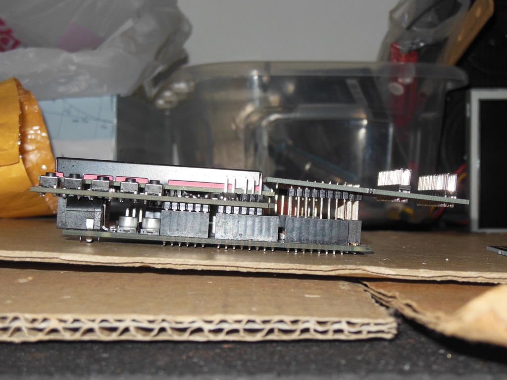
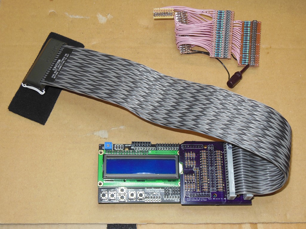
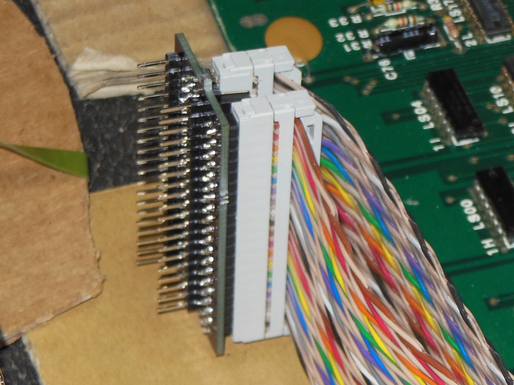
From a box of pods I pulled out a 1802 interface pod that has no known uses in the arcade world and more than likely little use
in the real world. This particular example looks NOS and still has the protective cover on the plastic.
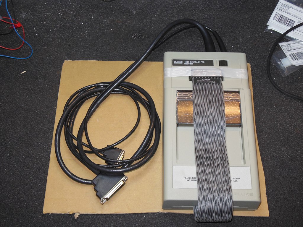

Investigating how the DIL pins of the pod cable were mapped to the twin IDC sockets revealed that each IDC connector is
mapped to one row of the DIL pins where one row of the IDC is the signal pins and the other is ground. Since the cable is
twisted pair this provides a signal/ground twist for each pin driven. Further, the ground pin for the CPU grounds all the
cable grounds in the cable. Unfortunately the 2650 has pin 21 ground and the 1802 has pin 20 ground so in order to use this cable
for the 2650 needs pin 20/21 swapped.
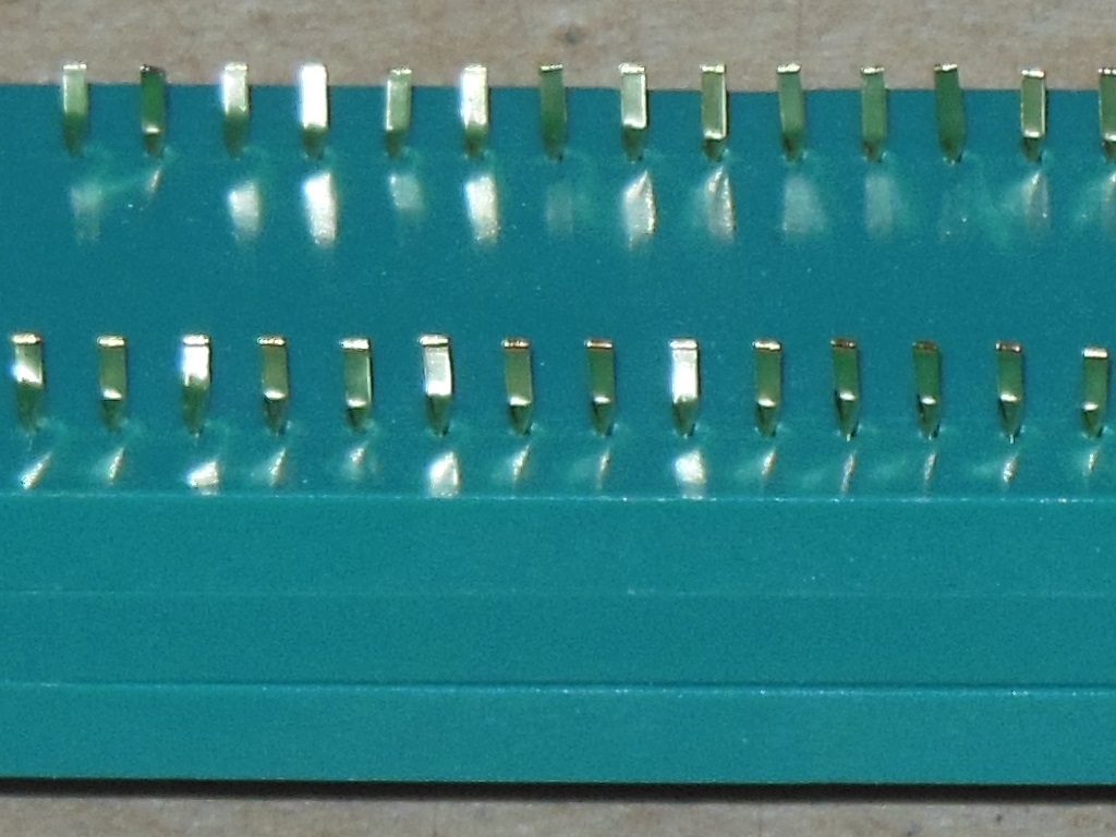
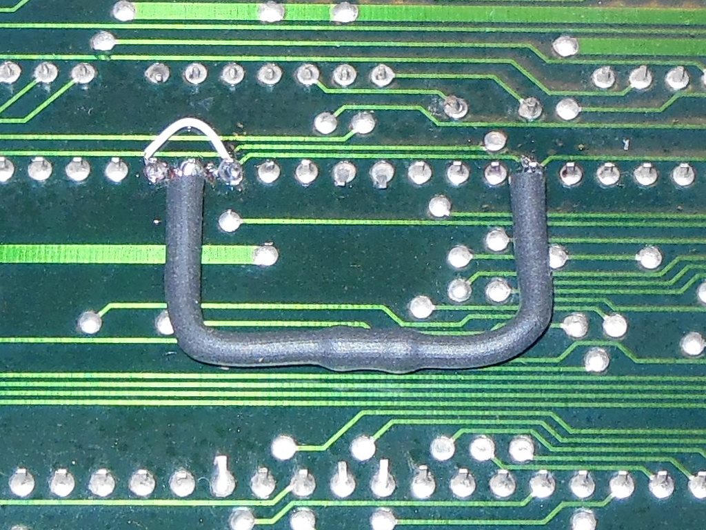
The pin swap for the tied ground pin in the Fluke DIL plug was straight forward since both pins are on the corners.
Pins 20 and 21 are bent out of a socket and then a short sold core wire crosses them to another socket, thus:
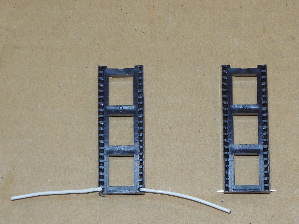
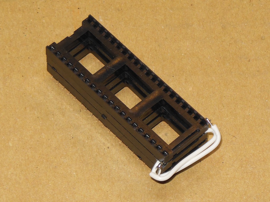
The swap is accommodated in the software portion of the project later on.
The consensus online is that the Arduino benefits from protective 470 Ohm resistor to ensure that a short
on the output pins doesn't burn out the device. Since this will be used on boards that are faulty and may
have bus shorts I decided to include the protective resistors in the wiring. The schematic is straight forward
- connect 40 Arduino digital output pins through a 470R resistor to the Fluke IDC signal connector. All the
Fluke cable grounds are connected to ground. In the prototype, I added a fly lead to connect the Arduino ground
to the Fluke DIL socket ground (the UUT ground).
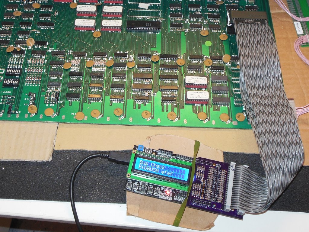
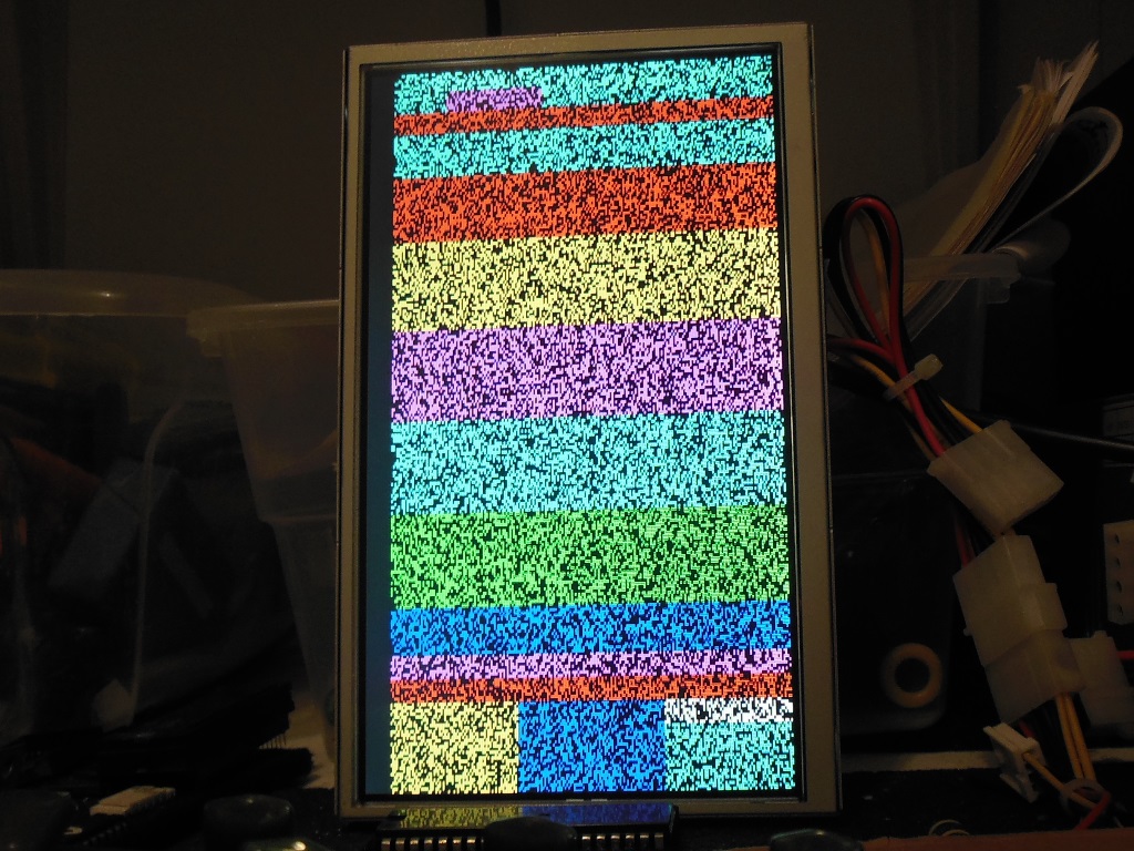
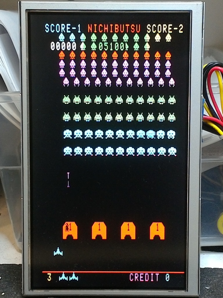
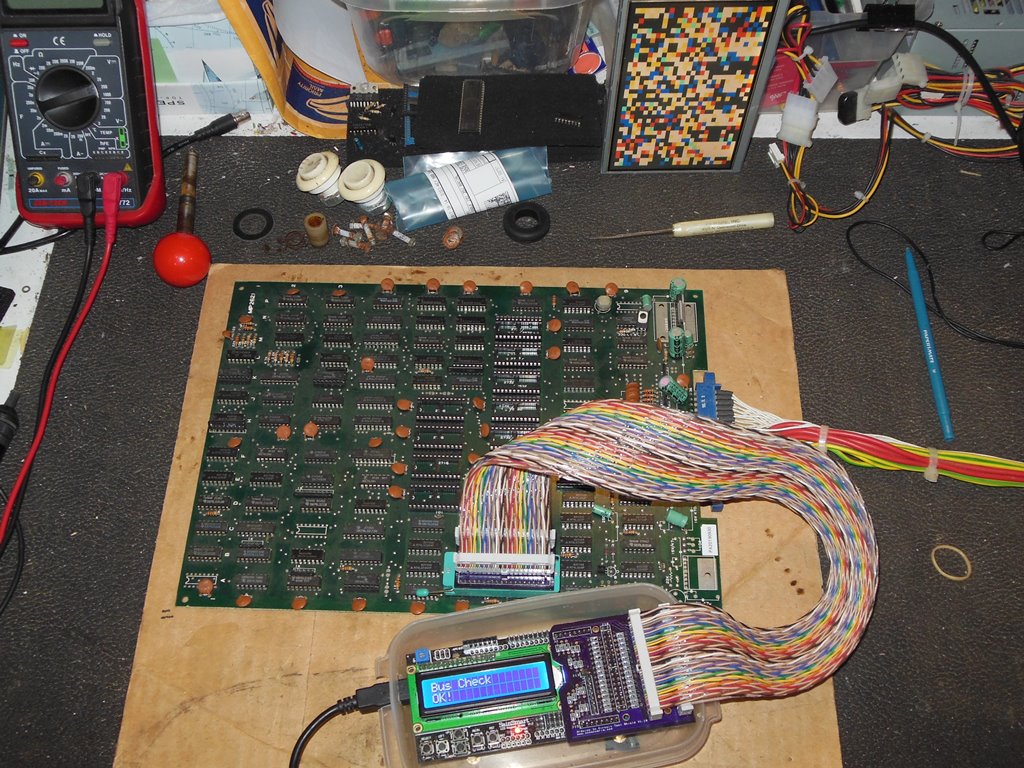
A mostly working Galaxia board was connected up and the basic connections metered out.
The first issue was that the software bus cycle complained that OPACK was already active at the start of the cycle. This turned
out to be that the Galaxia board ties OPACK active when anything other than the 2636 are accessed (i.e. the hardware never
needs to extend the bus cycle). A software revision adjusted for this behavior. ROM and RAM was accessible and working.
However the 2636 would not write/read reliably. This needed a bit of digging into the 2636 datasheet to figure out.
This is a much better timing diagram than the one from the 2650 manual. The key to my problems was on the read side
and the tDV timing in that the 2636 does not hold the read data on the bus indefinitely but only for a minimum of 2uS.
The software bus cycle was too slow to read the data. The fix for this was to optimize the cycle and the bus data
read to squeeze into 2uS. At 16MHz, this comes out to ~32 clocks. For an 8 bit bus, that's 4 clocks per bit. Some
creative optimizations managed to get the data bus read into 3 clocks per bit. Testing the 2636 had no issue after this.
The initial version of the software includes:-
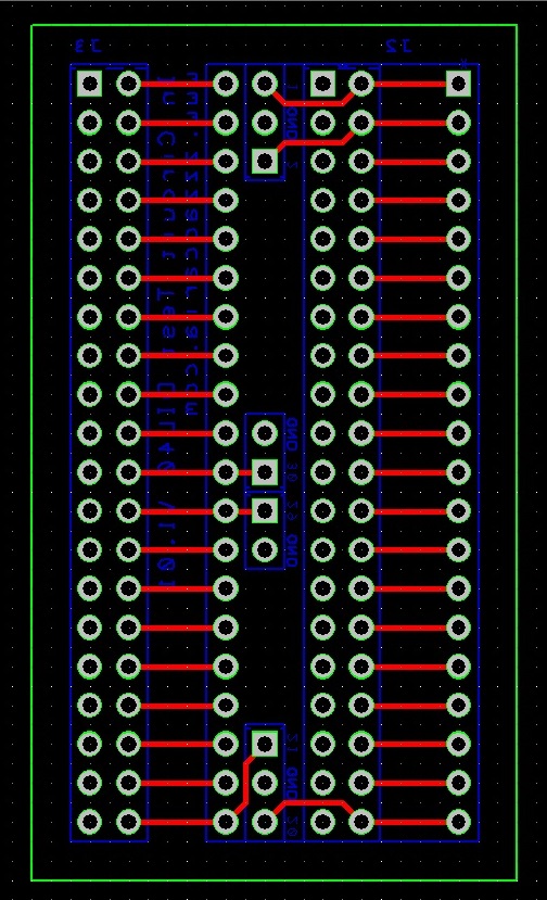
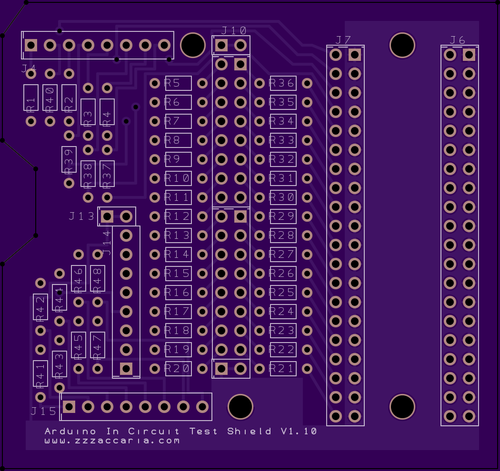
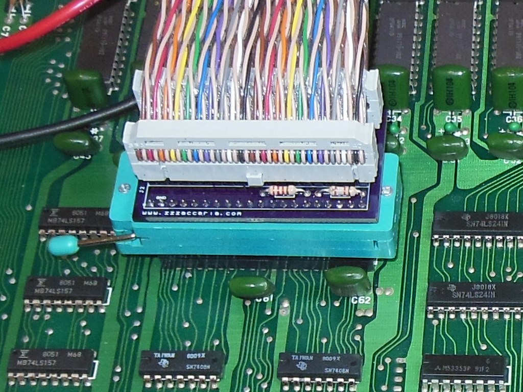
Since the prototype proved itself reliable and useful the next step was to design a production PCB for that comprises
both an Arduino "shield" and a DIL socket probe head so that the tester can be used without a Fluke cable and the DIL socket
probe head can be used to make a replacement Fluke cable. With that in mind, the probe head would need to be compatible with
several common microprocessors. Fluke probe head cables are slightly different for different microprocessors because the
ground pin is grounded in the probe head itself. The table below shows the differences:
| CPU | Vcc Pin | GND Pin |
|---|---|---|
| 2650 | 39 | 21 |
| 6502 | 8 | 1 & 21 |
| 6701 | 10 | 30 |
| 6800 | 8 | 1 & 21 |
| 6801 | 7 & 21 | 1 |
| 6802 | 8 & 35 | 1 & 21 |
| 6809 | 7 | 1 |
| 8035 | 40 | 20 |
| 8080 | 20 | 2 |
| 8085 | 40 | 20 |
| INS8900 | 25 | 30 |
| T11 | 40 | 8 & 20 |
| V30 | 40 | 20 |
| Z80 | 11 | 29 |
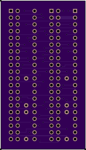
Several arcade folks recommended "Design Spark" for schematic
capture and PCB layout software. The plot output from Design Spark is not natively in the form OSHPark needs so it needed
a little bit of file renaming and settings changes to get the plot outputs right.

Shortly after sending off the PCB plots to OSHPark I realized that the final adjustment I did to increase the spacing
between the two boards to meet the OSHPark cut requirements had caused the copper pour areas to be misaligned on the
DIL probe head board :( The probe head board was ruined. What had happened was that the bounding box final move of the
whole probe head PCB had not moved the copper pour area. This was a bug/limitation (one of many) in Design Spark that
didn't support a simple move of a copper pour area :( The probe head board would need to be redone, however I chose
to wait for the ruined one to come back first to asses any other problems before trying a second attempt.
The shield PCB looked good for pin alignment but with the LCD shield on top of the Mega there was a misfit with
a protrusion from the LCD itself and the top left corner pin of the LCD shield.
To work around the protrusion I trimmed the corner and made a small cut-out in the shield PCB to allow it to sit flush.
Luckily there are no tracks in this area of the board to worry about but in future runs I'll adjust the shield PCB to
include the cut-out.
Assembling the shield was straight forward and there were no other issues discovered with it. The only things to note
are that the shield needs longer pins for the Arduino plugs to allow it to clear the LCD shield (I'm using 20mm ones)
and that all the resistors are the short form factor ones.
The production shield PCB has a slightly different pin out than the prototype and thus needed the control software updating
to use it. I'd also moved on to fixing an Astro Wars board and added that game to the tester along with other
software enhancements to aid with fault finding. Since the DIL probe head PCB was ruined I continued development with
the Fluke cable for now.
I was still having some reliability problems (unrelated to the shield PCB) that needed further investigation.
The 2636 read/write was still unreliable on Astro Wars. A further round of software optimizations didn't improve
the reliability and cross checking with the ATMega2560 device datasheet didn't indicate any possible cause. It was
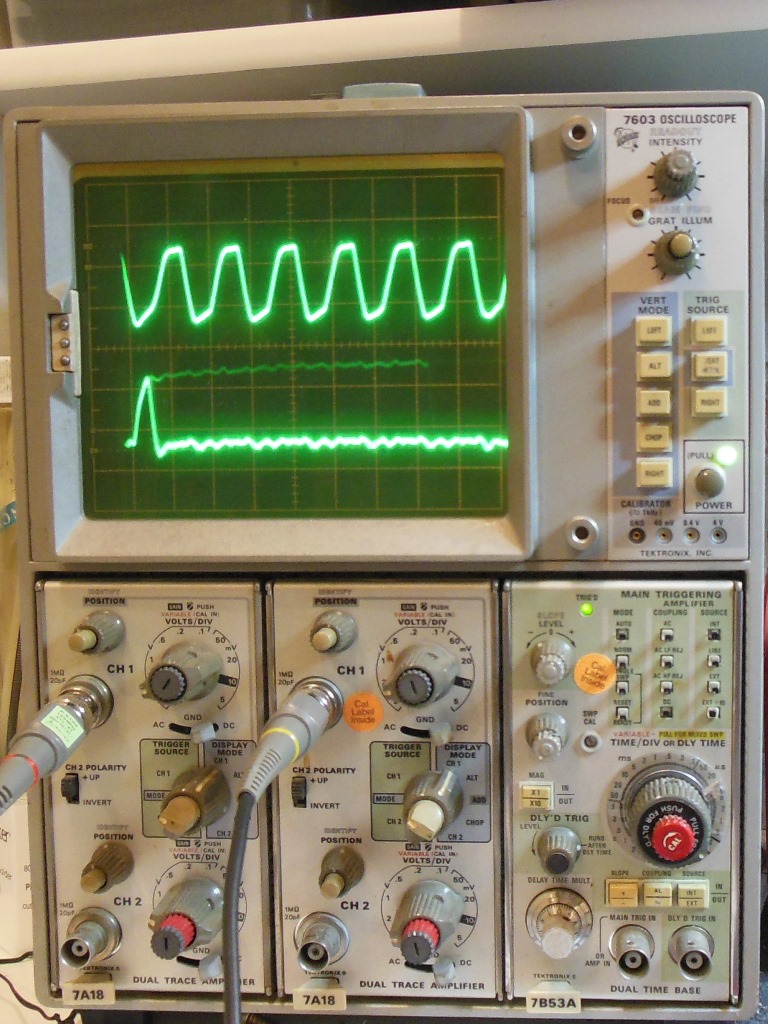
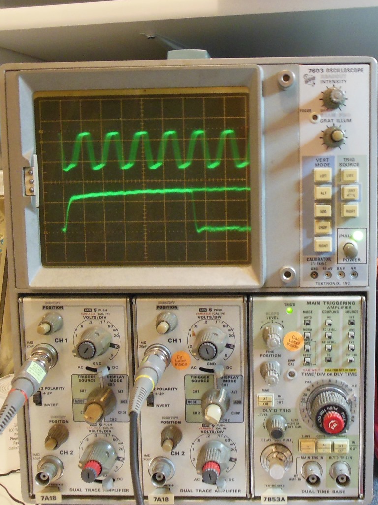
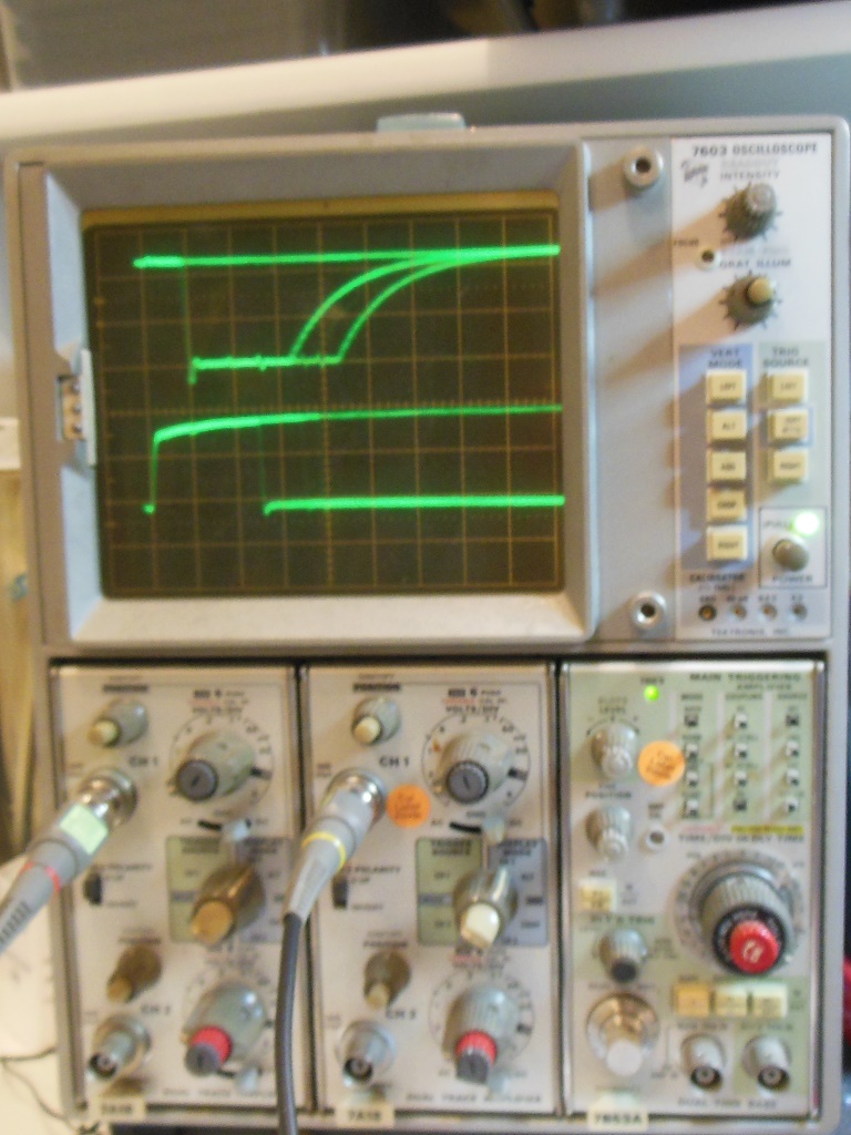
time to take a look on the scope. The pictures below show the 2650 in action, the first D0 and OPREQ and the second
2MHz clock and OPREQ.
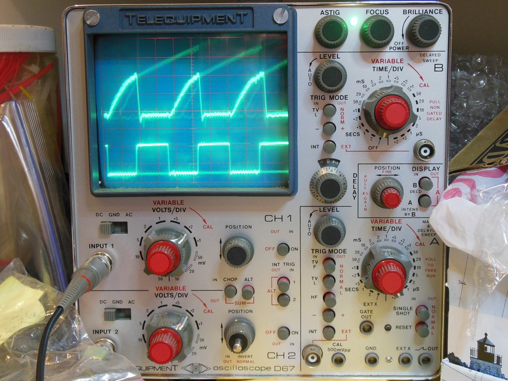
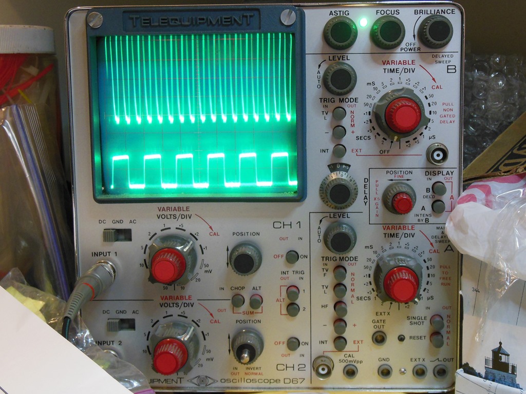
These pictures I compared with the Arduino software cycles and quickly found at least one issue - the software cycles
were much longer than the real 2650 cycles. A quick check only performing an OPREQ hi/lo (that should have been just a few
16MHz clocks) was taking around 24 16MHz clocks to be performed. With this in mind two conclusions could be drawn:
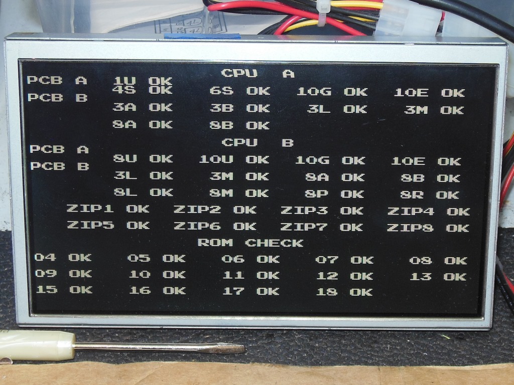
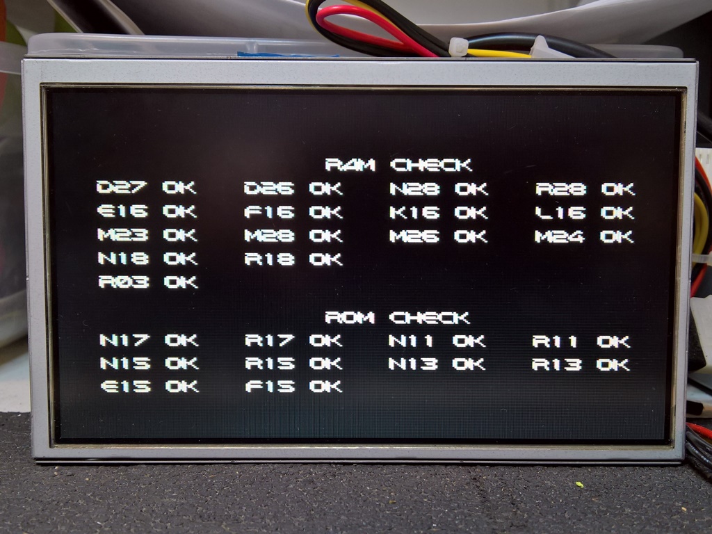
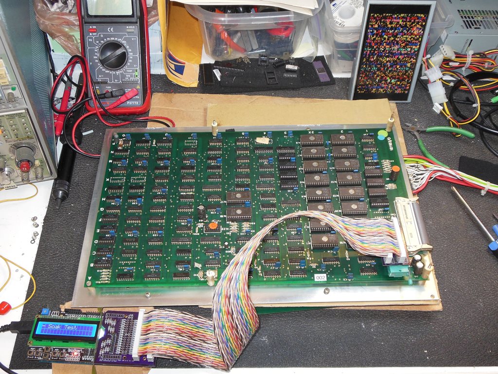
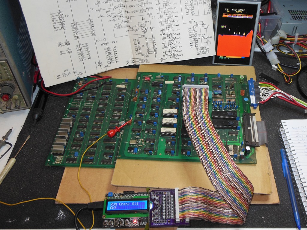
As part of the repair work on the Astro Wars boards I also added additional test options to the software to allow individual ROMs & RAMs to be checked (along with a few bug fixes here and there).
I used the ruined probe head PCB to make a mechanical mock up in order to verify the cabling and connector pin out. The pin out looked OK but there were some additional issues:


This time there looked to be no issues with the PCB and being only a small PCB was less than $15 to manufacture for 3:
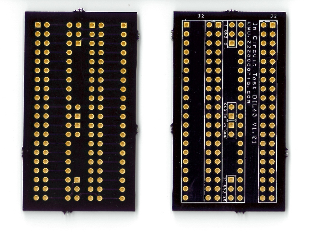
There were no physical issues at all with the redesigned probe head PCB. I made a set of cables (a pair 40-way IDC twisted pair
ribbon cables) based off slightly longer twist/flat ribbon cable. I wasn't able to find a source for the exact twist/flat length
fluke cable:
It functioned without issue or difference compared to the Fluke cable/probe assembly.
Since a few folks wanted some shield kits I decided to adjust the shield PCB to both separate it from
the the initial bad probe head plot and add in the cut outs for the LCD display shield:

A paper print-out confirmed the plots for the cut outs fitted properly:

Since I needed to fix a Tomahawk 777 board set (similar to Astro Fighter) I decided to code up the 6502 CPU.

The ROM read tests went OK but there were problems with the program RAM. I suspect this was because the 2114 chip select is gated by TCLD,
a quarter CLK2o pulse, that effectively halves the CLK2o high time to allow the address & data to setup on the RAM
for the 2nd half of chip selection. Since the tester pin drives asynchronously this type of circuit won't work properly with it.
The video RAM was even less reliable and wouldn't write/read 4 bytes. Looking more deeply at the schematics, it looked like the VRAM access for display occurs in the CLK2o low time with the CPU access in the CLK2o high time. Again, any external synchronization with the CPU input clock isn't going to work properly with simple pin drive. Thus, the tester can only be used reliably to validate the ROMS on this platform for now.
Since I needed to fix bad sound on Jackrabbit I decided to code up the Z80 CPU (hoping for better results than 6502 on Astro Fighter):
ROM tests were looking good (after some initial confusion over the "split" ROM memory map this platform uses). RAM tests were also looking
good with only an intermittent reliability problem with the background RAM. This platform uses a WAIT generator circuit
that's synchronized to the CPU input clock so the tester was encountering WAIT's in the wrong places. This circuit is only triggered for writes
to the background RAM where the WAITs are used to hold the CPU until the next HBLANK period. I used a small workaround in the Z80 CPU code to
explicitly use the WAIT signal to synchronize the start of the cycle with the start of HBLANK for accesses to this region. This fixed the issues
as far as I can tell. I also added code to setup the 8255 for reading the inputs and dip switches and actually used the tester to find the sound problem,
a stuck output on the sound latch, in only a few minutes :)
I needed to fix a G.G.I Corp Galaxian bootleg board to use for a Macro's Galaxian Multigame setup so I added support
for that to the Z80 configuration:
Similarly to the Jackrabbit board, access to some portions of the video RAM required WAIT line pre-synchronization for
video blanking and the same workaround in the Z80 CPU code for Jackrabbit also worked for Galaxian. Since I wasn't sure what this bootleg
was converted to I refactored the interrupt code to be able to properly test that the board was working as a Galaxian game (NMI vs IRQ).
This was the first board that actually failed the interrupt test due to a fault in the video counters that caused no
trigger of the interrupt. The board had several issues - both 2101's bad, one 2114 bad, one 8216 bad and both LS161 vertical counters
were bad. After repairs, a complete pass of all the ICT tests (except ROM since I had none installed) was confirmed with the
multi-game working first try without major issues :)
Since I was working on repairs to a US Billiards Quasar machine I decided to add Zaccaria Quasar support to the tester.
This platform uses bank switching so I needed to implement bank switch handlers to be able to have the tester get to all the memory
on the board. Unlike Astro Wars/Galaxia the shell memory is not readable so I needed to introduce a "Write Only Memory" concept
to be able to add some support for testing that. I also added some additional memory write options to be able to clear all the memory to
a known value that was needed to initialize the PVI's and allow the graphics to display (the uninitialized PVI's caused the screen to
be all white masking all the other graphics output).
The particular board I was using to bring up the tester had one bad 2114 effect RAM, all three 2102 colour RAMs bad (one dead, one with a bad row of bits and one with a single bit bad) and a bad ROM socket. With all tests passing with the tester, with a real 2650 the board would reset starting attract mode or get into attract mode but with all or part of the scrolling title missing. Despite a lot of poking around with a scope I wasn't able to determine the cause - likely it's an analogue issue with slow access time or bad logic levels that the tester doesn't trip over but the real CPU does. Shelved this particular board for now.
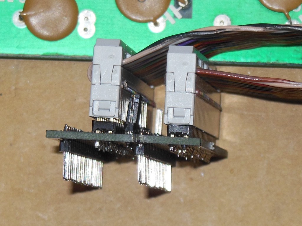
I was asked about the probe head assembly and how to properly use that with CPU sockets. Since the probe head uses standard pin headers
they are square and thicker than IC pins. Therefore, using these pins directly in a CPU socket would sprain the socket. Further, plugging
and unplugging to fit a real CPU for testing is additional wear on the CPU socket. To alleviate both of these problems I use a ZIF socket
fitted into a normal CPU socket as a bridge between the probe head header pins and the CPU socket on the PCB:
The ZIF socket pins themselves are orientated the wrong way and thus each ZIF socket pin needs a 90 degree twist applied to it with a
pair of long nose pliers ~1mm up from the ZIF socket body. This makes the pins match the usual IC pin orientation and allows the ZIF
socket to plug easily into an Augat 40-pin DIL socket. The pins on the Augat sockets match IC pins pretty closely - they are slightly
thinner than IC pins and thus they tend to exacerbate loose/bad CPU sockets that would need to be changed anyway.
I had some Atari Star Wars game boards based on the Motorola 6809E CPU that I needed to fix. From the previous investigations on the
6502 CPU I already knew that this was a clock-synchronous design and thus wouldn't be usable with the ICT as is. I had a Fluke 9100A with
a 6809E CPU pod that I could use instead and the boards I had all had math errors so I planned to use the Fluke if needed. As I started
working on the boards on the bench I realized that there were some diagnostic challenges with the game. First, the Atari self-test
only has two options - run all the tests repeatedly (the normal test mode) or run a single test once after reset (the option switch
diagnostic mode). What I really wanted was a single test repeat and there didn't seem to be a way to have the built in tests do that.
Second, the matrix multiply and accumulate circuitry is serial in nature making it awkward to trigger and capture on a scope to validate
the serial data streams. Thirdly, using the Fluke to program the math boxes would need some Fluke scripting magic or a lot of manual
programming to set them up. Thus I could see significant diagnostic benefits if I could get the ICT to work with this platform.
As with the 6502 the central problem is that the bus cycles of the CPU are driven externally by an external clock (two clocks for
6809E, "E" and "Q"). Looking at the Star Wars schematics I saw that the whole game was driven from a single 12MHz master clock.
The plan was to disconnect the 12MHz oscillator circuit and instead drive the master clock from one of the auxiliary pins on the ICT
daughter board. Driving the clock this way would allow the tester to output proper "E" & "Q" synchronized 6809E bus cycles by toggling
the master clock and sampling "E" & "Q" for the proper signal phasing for the bus cycles.
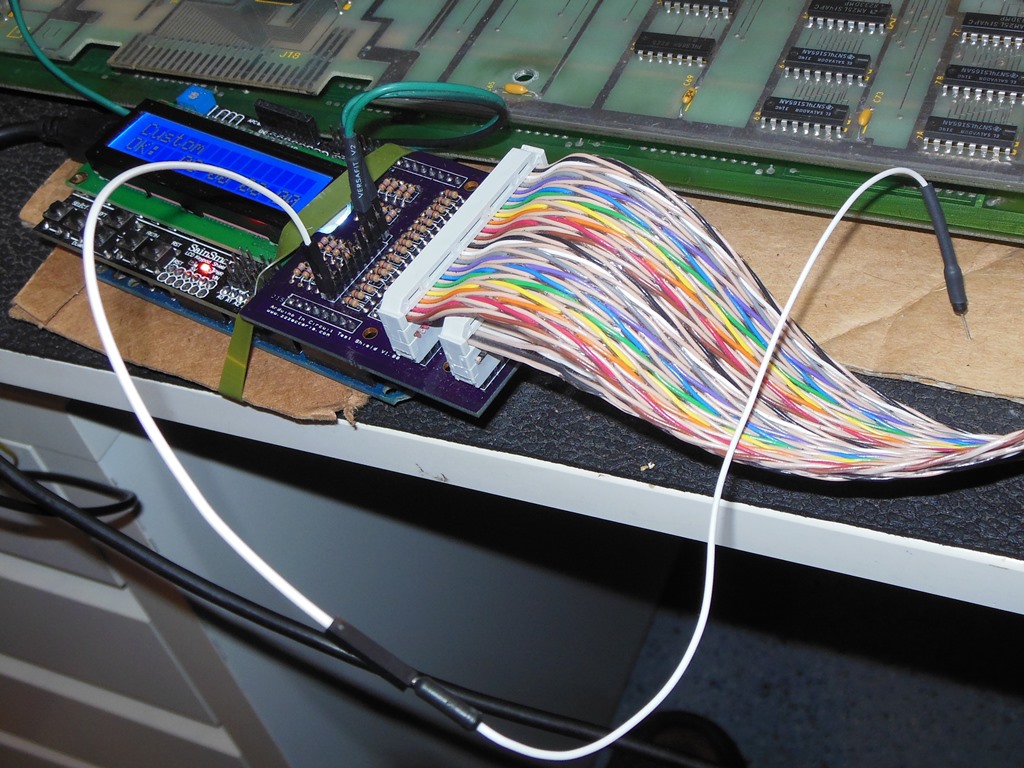
I hadn't previously fitted the pin headers for the spare port on the top of the daughter shield so did that and made up a cable to
connect it to IC clips to attach to the board under test (ground & clock).

To connect the clock output from the ICT as the master clock input I removed the IC 1N (74S04) and fitted a socket. The replacement '04
was then fitted in the socket with pin 1 angled out of the socket to disconnect it from the oscillator and allow the IC clip to be
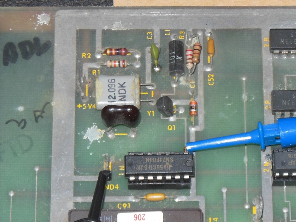
attached to the pin instead. The ground pin can be attached to the GND4 ground test tab. Some boards don't have the GND4 tab fitted so
an alternative location for the ground connection is the left pin of capacitor C91.

Since the ICT doesn't support running the actual game, to go back to the game configuration needs the CPU fitting and the master
clock reconnecting to the 12MHz oscillator output transistor.
The Star Wars trouble shooting guide contains a very detailed description of the math box tests that was enough information to implement
"Custom" functions on the ICT to execute the same tests (tests 10 to 25). The ICT test results were exactly the same as the Atari
built in test functions for the (faulty) board I was working with.
With the ICT in control of the master clock I added another "Custom" function to perform a single clock pulse. This allows the math
circuitry to be be "single stepped" forward to allow easy investigation of its operation.
The second benefit of the ICT's control of the master clock was the ability to use another one of the auxiliary pins for sampling an input
signal. I added another custom function that sampled this pin for 32 clock pulses and displayed the result on the ICT. This allows easy
capture of the serial streams in the math circuit - for example two 32 clock captures (64 clocks total) is enough to capture a signal for
the whole sequence for the simple built in matrix self-tests. The captures not only make it easy to see the serial data in the system but
can also be used as a quick reference against "known good" captures. I've started adding these captures to a file for future use:
Star Wars captures
The time investment paid off - I was able to diagnose the matrix problems on two boards in less than 10 minutes:)
As noted previously using the ICT with the Astro Fighter platform proved mostly unsuccessful however using a clock mastering configuration
had worked OK for 6809E with Star Wars so I decided to try implementing an alternative 6502 clock master configuration for use on this
platform. It was still useful to keep the original asynchronous 6502 implementation around in order to test the sound & video controls
so this new 6502 clock master configuration is side-by-side with the original.
The theory was the same as it had been on 6809E - drive the game master clock in place of the crystal oscillator output from a spare pin
on the ICT and then implement the 6502 synchronously from the master clock input.
There was one complication with doing this on the Astro Fighter platform - the game uses DRAM that has refresh time constraints
that the ICT may not be able to honour due to the slower clock input. In testing on the board I was using the full 8Kb RAM test almost
passed but had a single bit error in one test. Splitting the DRAM into two 4Kb halves gave a consistent passing RAM test.
Having reached my last working Phoenix board leaving a box the none-workers to fix I decided to add support for the Intel 8085 CPU and
Phoenix. The implementation of 8085 is similar to Z80 with the principle difference being the multiplexed address/data bus.
The Phoenix platform doesn't use any of the unusual features of the 8085 and is fully asynchronous. The implementation did need a READY
synchronization workaround for proper video RAM sharing however.
A community member requested the addition of support for the DEC T11 CPU as used on the Atari System 2 platform (Paperboy, 720, Super Sprint, Championship Sprint, APB). The CPU is a a bit of an odd-ball since it was originally intended for enterprise microcomputers compatible with VAX mainframes. Like the 2650, there is no Fluke pod available for it.
The first key complexity was that the T11 is a 16-bit CPU. This necessitated a lot of software work on the tester infrastructure to expand the CPU class to 16-bit data and define 8-bit & 16-bit width access indicators. It also needed all the test libraries (ROM & RAM tests for example) enhancing to be able to test 8-bit & 16-bit wide devices including handling byte addressability. The T11 itself is also awkward in many ways compared to other CPU's. All in all it ended up being quite a pain to sort it all out to at least a basic RAM, ROM & IO test level.
A friend loaned me a Super Sprint board set to use for testing. The first step was to validate a simple ROM test of the "fixed"
ROM and RAM. The next step was to work around the complicated bank switching arrangement Atari used to shoe-horn the "paged"
program ROMs into the limited address space. The program RAM is unpaged and thus can be tested conventionally. The CPU board can
be conveniently tested alone without the large video board attached.
Moving on to attach the video board, after solving the subsequent power distribution problems using it introduced, allowed for
implementing a video RAM test.
Testing the video RAM also has complications - it's bank switched via the Slapstic copy protection and arbitrated with
display using "clock stretching" of the T11 input clock (why Atari didn't use a conventional READY based bus wait I haven't dug
into). The bank switching I ignored for now, figuring the built in self-test
would be sufficient for diagnostic. The arbitration problem wasn't going to be something that could be solved in the same way
Atari did using "clock stretching" given the pin drive nature of the tester. Instead, I implemented support for the VBLANK
interrupt and used that to synchronize access to the VRAM so as to always ensure access was performed at a time when no
CPU hold off occurs. The disadvantage of this method is that it limits VRAM access speed to ~50 cycles per second that thus slows
the RAM test down such that it takes several minutes for the whole bank.
The arcade community contributed support for the Motorola 6802 CPU and the Williams Sound Board as used on various pinballs and the Defender et all series of video arcade games. Along with that support also came some useful utilities for generating the ROM descriptions from ROM images.
The arcade community contributed support for the Williams Defender platform based on the existing clock master implementation of the 6809E CPU. This platform has 48Kb of DRAM and thus potentially incompatible with clock mastering, however testing indicated that it worked OK.
A community member requested support for the Intel 8080 CPU in order to fix some Space Invaders boards. The 8080 uses
a triple rail power supply and runs off MOS (12V) level clocks so the generic probe head would not be safe to use as-is for
this CPU.

I started out by building a new generic probe head that had the four none-TTL voltage pins (11,15,22,28) isolated by track
cuts making it safe to use with the Arduino. On the software side, the implementation of the bus cycles followed the same
pattern as prior implementations and yielded good results for ROM, inputs & outputs but did not work at all for the DRAM.
Given that DRAM issues are a major fault area on Space Invaders, the tester would not be too useful with DRAM not working.
To figure out what was going on needed a close look at the 8080 bus cycle timing and the Space Invaders schematic.
The datasheet timing diagram is not the clearest on what's going on but the key point was that the DRAM cycle is triggered
by the SYNC signal, held with READY and then cleared on the clock cycle after READY is de-asserted. With the tester running
asynchronous and without any adherence to the actual low level bus timing the DRAM wouldn't work :(
I'd previously encountered this problem of clock synchronization on 6502/6809 and partly on Z80 with WAIT and worked around it with clock control or specific platform handling. Neither of those options looked viable on this platform necessitating further investigation. One idea was to try to instruction level optimize the Arduino code to be able to match more closely the actual bus timing. This boiled down to:
The 8080 dedicated probe head optimally groups the pins and adds four resistors for a potential divider to adapt the two
MOS (+12V) clock inputs to TTL. Using the minimum track width & via sizes OSHPark design rules stated the dedicated probe head
was only just able to remain the same minimal size as the generic probe head.

The PCB layout I completely manually routed (the built in auto-router was not able to fully route the board).

Based on prior experience I also checked OSHParks estimated board appearance to make sure the plotting had turned out looking OK.

The boards came back from OSHPark and thankfully looked OK. The first task was to calibrate the two clock potential dividers
to make sure the Arduino wasn't damaged before plugging it in.
The initial calculations I made we're slightly off because I forgot to account for the clock inputs being less than 12V
both due to a 150R series resistor on the main board and lower output voltage from the clock generator. The second attempt worked OK.
With R1=2.2K, R2=1.8K, R3=2.2K, R4=1.8K then the current I=3mA @ 12V.
For a given input the potential divider outputs:-
At 12V in 5.4V out
At 8V in 3.6V out
With the 150R in series on the main board, at 12V input the output becomes 5.20V.
Confirming with a scope showed that the voltage levels looked safe & reasonable but the potential divider makes an RC filter with
stray capacitance causing the clock to become more saw-tooth like. This did not appear to affect the tester significantly, however.

With the optimized software the DRAM worked reliably and I tuned the bus cycle code using the scope to match the 8080 datasheet as
closely as possible based on the Nichibutsu Moon Base 3-board set.

I quickly discovered that the existing basic write-random and read-verify sequential RAM test was not thorough enough for the
DRAM used on this board. At least two CPU boards passed the original ICT RAM test but were crashing with a real 8080 CPU
installed. To address the more peculiar failure modes of this flavour of DRAM I wrote a new random access RAM test for use
only with byte-wide memory, "RAM Check All RA". This test performs a more realistic set of memory operations closer to the
behavior of a real CPU - writes, re-writes, read-verifies, clears, pauses etc. across the whole of the memory block at random
address. This version of the RAM test was able to reproduce DRAM failures on the two boards that passed the simple RAM test.
With the enhanced RAM test and the existing test software for inputs & outputs I was able to get my two boards in good shape,
working through the sound issues common on the Space Invaders platform. However, I had one Moon Base set that wasn't working
properly despite passing all the usual tests.
I suspected a bad shifter circuit, that on Taito boards is often a Fujitsu single IC but on Moon Base is implemented in
discrete TTL. Using MAME source as an explanation of the shifters function I added a custom test to the ICT to validate
that the shifter was working. It wasn't, and the ICT function left the shifter in the failing state making it easy to find
the bad IC's (two in this case). The repairs were finally complete!
Links to order the 8080 dedicated probe head PCB are at the bottom of the page.
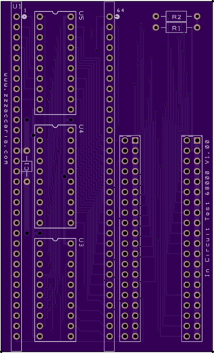
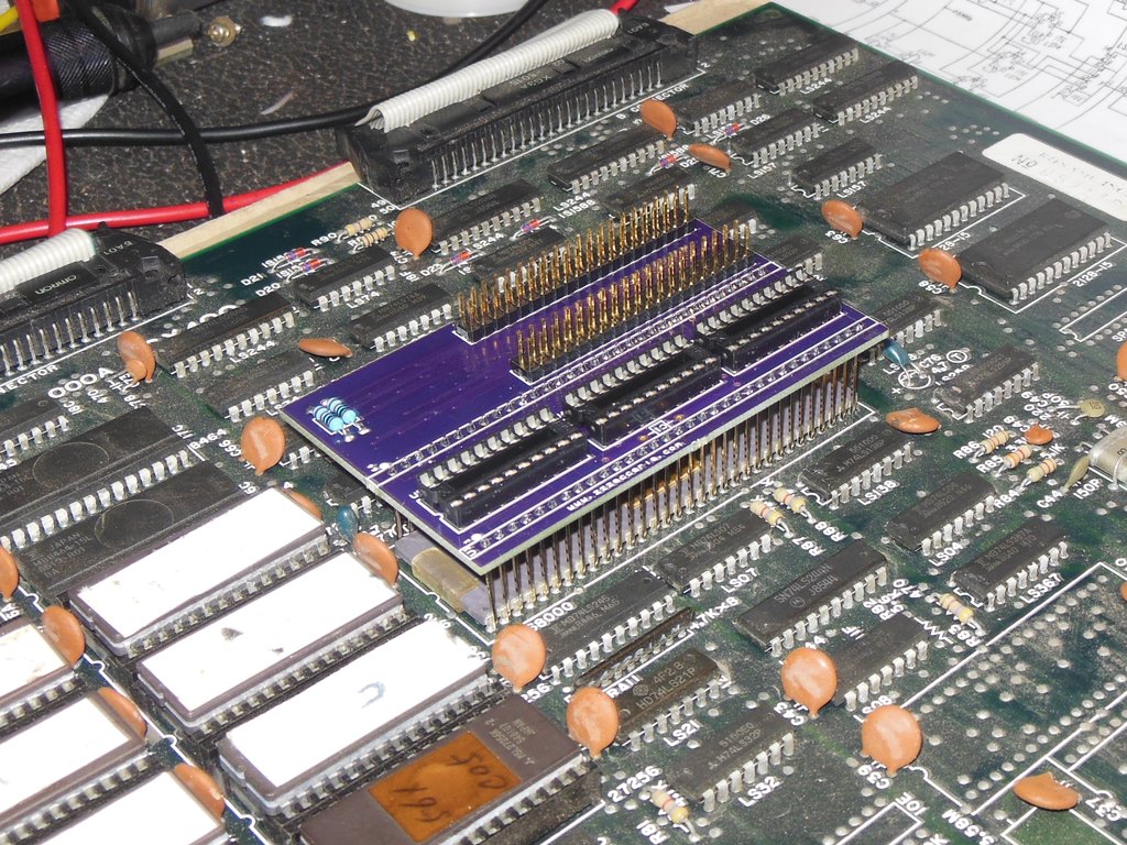
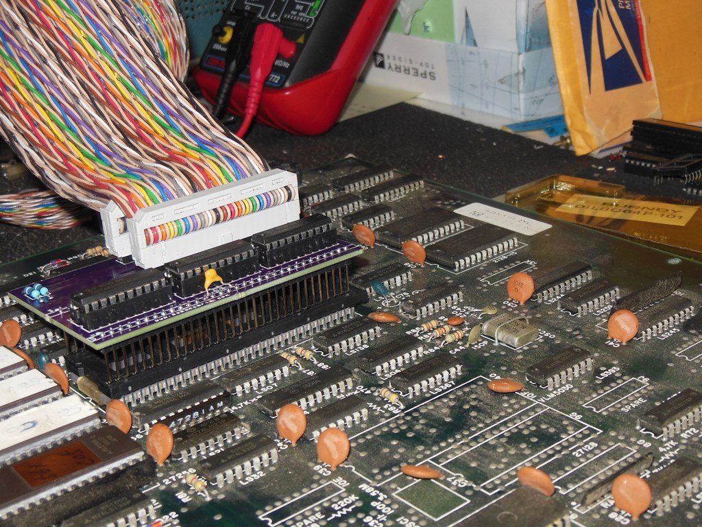
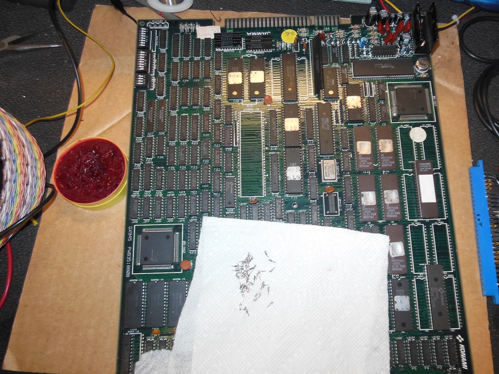
A fellow collector requested help repairing a somewhat rare non-booting Gradius III PCB. I started out intending to use my Fluke 9100 and 68000 pod for this repair but discovered that neither the main 9100 chassis or the 68000 pod were working now (it'd been a few years since I'd last used it). I faced the choice of repairing the Fluke setup or pursuing trying to implement 68000 CPU support using the Arduino ICT. I decided to have a shot at the latter but it was pushing the bounds of its capability given the 40-pin limit and 16MHz Arduino clock versus the 10Mhz of the 68000 used on these games.
The first step was to design a dedicated 68000 probe head PCB. This one needed to translate the 40-pins of the Arduino ICT into the 64 pins that the 68000 requires. The 23 pins of the address bus could be mapped to three 8-bit latches that then left only 2 pins to find a home for (after also accounting for the 3 address latch controls and address output enable). The two pins chosen to not map through were the 'BG' and 'BGACK' pins since the tester would not be able to support bus sharing and it didn't look like any games used that feature of the CPU. These two unused pins I pulled high with 10K ohm resistors on the probe head. I also added a 1uF ceramic capacitor across the power & ground for the three new IC's.
Making the probe head PCB as small as possible was a priority for the layout to minimize the area of the game PCB obscured by
the probe head - the larger the probe head the more difficult it is to probe IC's that are close to or underneath the probe head.
Thankfully the 68000 is a large package and the three latches were able to fit in the middle of it but there wasn't enough space to
also squeeze in the cable connectors. Even in this footprint it necessitated using the Osh Park minimum allowable spacings and
track widths to be able to route the board (allowing two tracks between pads).

The PCB manufacturing check images yielded a couple of bugs with some of the silk screening being on the wrong layer that I needed
to fix but otherwise they looked good to go.
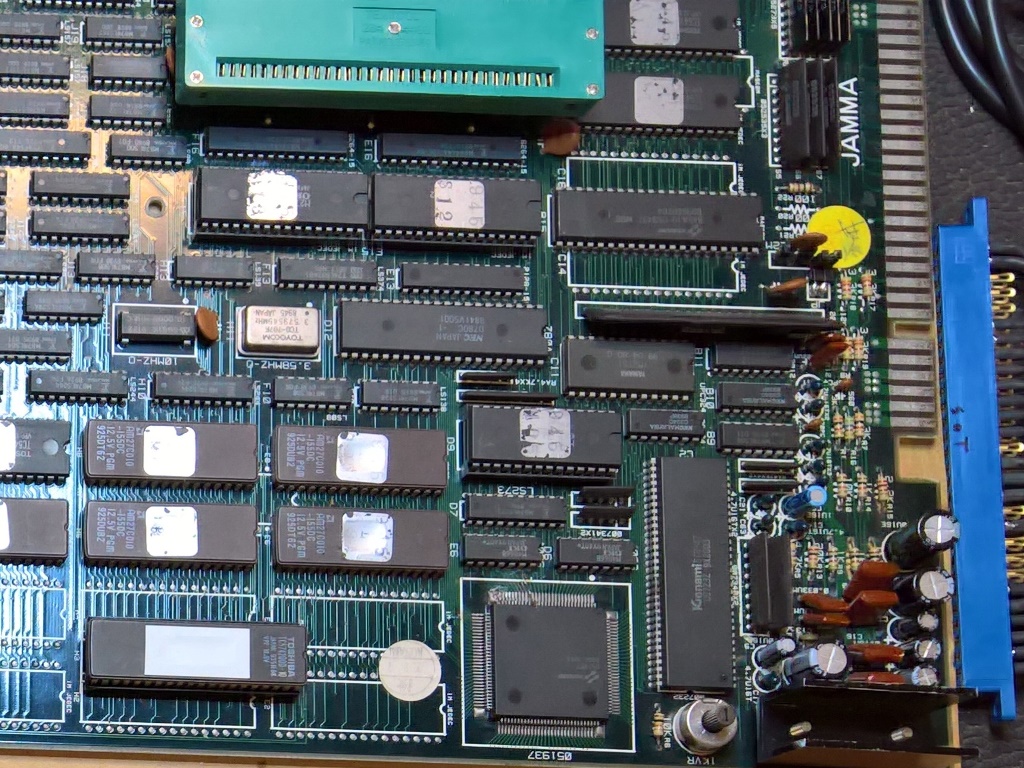
I selected Konami GX400 (used for Konami GT and Nemesis) as the target platform for bring-up of the 68000 ICT. It's an early
popular single CPU game that I have in both games with readily available schematics for ease of debug.
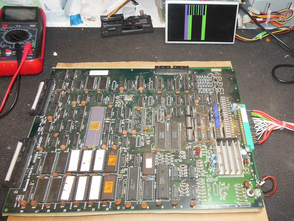
There were already unexpected problems that needed to be solved. Firstly, the game I had didn't boot which meant that I would need
to debug the tester and debug the game at the same time. Secondly, the 68000 CPU wasn't in a socket and the one in there was
a nice ceramic example of the 68000 that would be a shame to have to cut out if it wasn't bad. Thirdly, the game has a watchdog that
would need to be disabled. Taking the easy one first - disabling the watchdog - looking through the schematics showed an unlabeled
jumper connected to a custom IC that was also involved in the reset circuit.
I suspected that this jumper was related to disabling the watchdog circuit since pin 4 was the RES (reset) output line. On the PCB itself
I tracked this jumper to a pair of pads near the audio amplifier heat sink labelled "JP1".
For ease of use I fitted a 2-pin L header pin connector to allow a jumper link to be used to enable & disable the connection.
Testing out the RES line proved that my suspicion was correct - fitting the jumper link disabled the watchdog. I later discovered
that this design was consistently used in later Konami games for disabling the watchdog - a similar pair of pads existed on many games.
The next problem to solve was the lack of a socketed CPU. The 68000 was originally designed as a powerful 16-bit replacement for
older generation 8-bit CPU's and as such has good support for bus sharing for multiprocessor and peripheral direct memory access
designs. Buried in the 68000 user�s manual was the table I was looking for covering bus sharing pin state.
The bus sharing state is controlled by 'BR' (Bus Request) to which the CPU responds with 'BG' (Bus Grant) after floating most of the
bus pins. The table above shows that all the bus pins are either input, open drain or floating during 'BG' except the
6800 peripheral 'E' clock. The 'E' clock isn't used on the Konami GX400 platform, so it looked like the ICT probe head could be used
leaving the original CPU in place and by having the tester drive 'BR'.
The Konami GX400 schematics show that the 'BR' signal pin 13 is tied high to +5V. In order for the tester to override the signal to
drive it low the board needed a small modification to instead make 'BR' a simple pullup.
The row of three pins tied together are 'BGACK', 'BR' and 'Vcc' so in order to fit a pullup necessitated cutting the two links,
adding a wire strap to reconnect the two outer pins and adding a 10KOhm pullup resistor from 'BR' to Vcc.
With the watchdog and bus sharing understood and taken care of the next problem to solve was how to mechanically connect the ICT
to the existing 68000 CPU on the board. Initial attempts at just sliding the pins over the top was nearly impossible due to the ICT
pins sliding off to the side between the CPU pins. Using much shorter ICT pins would have kept the pins in place but would be too rigid
to clip over and connect.
The 0.9" wide 64-pin package is unusual and difficult to source parts for. I considered using a socket since sockets have flatter pins
but the standard DIL sockets I had didn't easily accommodate the larger pin header pins on the ICT. I then tried using a ZIF socket,
a Burndy DILPQ64P-101, that I found on eBay.
The ICT pins fit tightly in this socket due to the larger holes that accommodated the ZIF action. It looked perfect, however it didn't
work electrically - the ICT pins were not contacting ZIF socket pins. I accidentally found the real answer - the ZIF socket is open
at the bottom so the ICT pins could be pushed all the way through the ZIF socket to land on the CPU pins. The ZIF socket acted as a
"guide" for landing the ICT pins and this was the best solution I could come up with for the mechanical attachment of the ICT to the
CPU.
Initial software implementation of the simple bus cycles proved problematic. Nothing really worked reliably and the implementation
needed to be as optimized as possible, close to assembly level, with minimal instructions.
The problems with ROM read root caused to actual bad ROMS :) Replacing the bad ROMS not only fixed the ICT ROM test but also brought the
game to life. Since the 68000 was still present, a simple reset of the ICT allows it to run after reset (hinting that in future I should
be able to add a "Run UUT" like function to the ICT).

The ROM test and basic program RAM test looked good but as has been the case with other games access to the shared video RAM was
problematic. Konami used 'DTACK' to extend the cycle for video RAM access that also used synchronous completions for the cycle (i.e.
DTACK is asserted but the data is held on the bus for a limited time). Writes appeared to be working reliably but hitting the read window
was not. No amount of software optimization could hit it. Looking at the oscilloscope traces showed that the signals had very slow edges
as a result of the shield protection resistors so I built a shield without those to test out.
With the shield protection resistors removed the oscilloscope traces looked much better and the reliability of the video RAM testing was
also much better but still not 100% reliable. This was as close as I could get and would have to be a known limitation.
The next investigation was to try out a Konami dual 68000 Dark Adventure PCB, also known as "Twin 16". This one had a plastic package
68000 rather than the ceramic package of the Konami GT but the ICT was still able to fit OK using the ZIP socket guide scheme. Unlike
Konami GT, however, Konami had fixed the hard connection of 'BR' to +5V and instead used a pullup so no track cuts were required -
plug'n'play :)
This platform runs at a higher clock rate than Konami GT and another round of software optimizations were needed to again get close
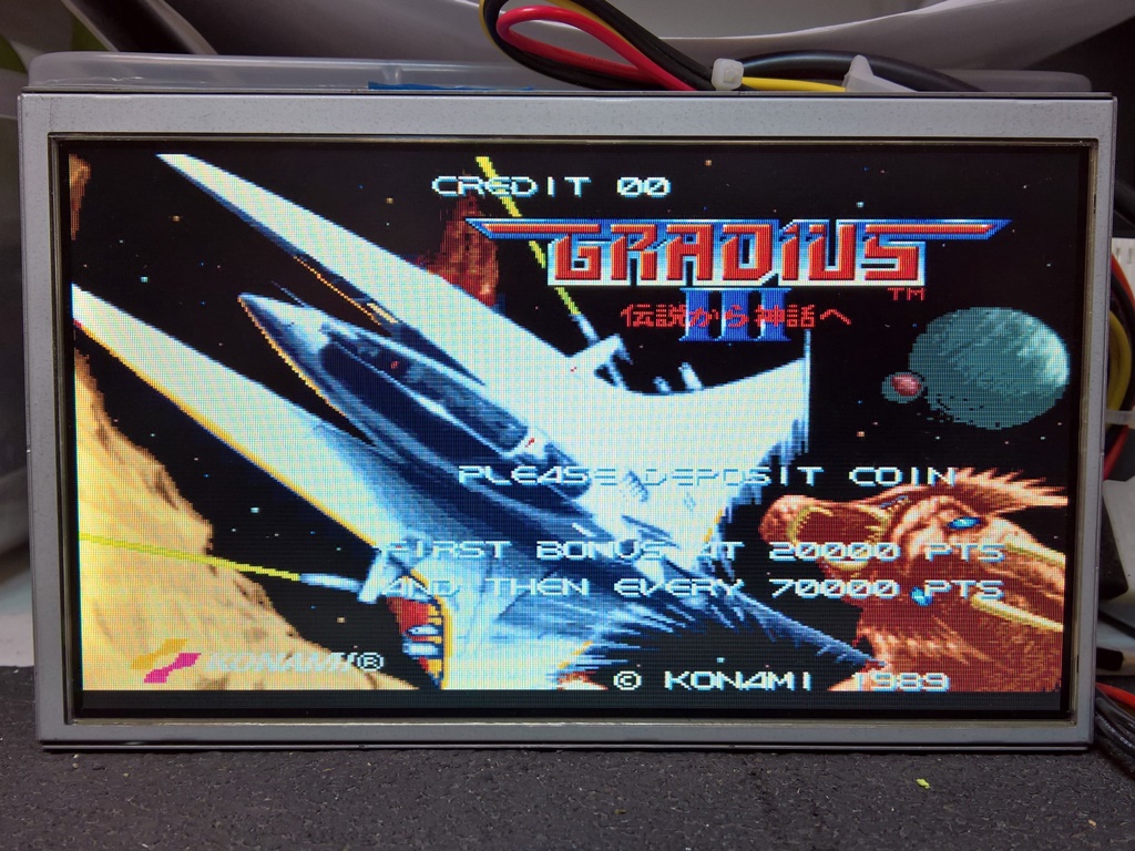
to being able to access the VRAM. The PCB I was testing with didn't appear to be faulty but I kept a picture of the self
test screen as a future guide to what was where.
Finally on to the none-booting Konami Gradius III PCB. Sharing a lot of similarities with Dark Adventure in being a dual 68000
based game it didn't share the same convenient pullup of 'BR' as that game :( Further, the PCB is 4 layer with full power and ground
planes such that the 'BR' pin had no track and sank straight into the power plane. The high packing density of the board didn't leave
enough clearance to be able to even side cut the pin on the 68000 to strap it. I decided to remove and socket a new 68000 CPU to start
with.
The CPU was replaced with a standard socket into which I plugged in a traditional 3M TEXTOOL ZIF socket (there was still one seller
on eBay that sold 0.9" 64-pin ZIF sockets). This board like the other two had a pair of pads to attach a pin header for the watchdog
disable jumper.
ROM test & program RAM test passed OK so the focus became the state of the video RAM. As mentioned above, the video RAM testing
is not 100% reliable and therefore some care was needed to understand where things were. In this case it was straight forward -
even a simple 4-byte write/read test wasn't working to one of the RAM blocks. Probing with a scope found that the RAM could be
read but no writes to them were occurring (the write pulse itself was missing). The write pulse from the RAM tracked back to
floating outputs on a pair of 74LS32 that were gating the 68000 write signal. It sounds simple but this all had to be done
by time consuming reconstruction the circuit with a multi-meter due to the lack of available schematics for this game.
Replacing the 74LS32 brought the game to life with a passing self-test :)
Links to order the 68000 dedicated probe head PCB are at the bottom of the page.
I had a couple of SNK Arian Mission PCB's to start with, out of which I hoped to get one working set. The platform is a twin Z80 based
system for which I could find no schematics. A scan of the MAME driver revealed a few SNK games on similar hardware and I was able to
find a very poor scan of Marvins Maze schematics to gain a general idea of how it worked.
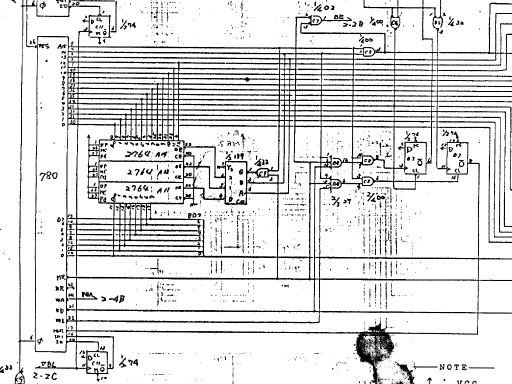
The schematics hinted that one Z80 is master and the other is a slave. WAIT synchronization appeared to be only used on one of the Z80's
(i.e. one Z80 always waits for the other) and I wasn't able to determine any obvious video RAM synchronization. That being the case, it
looked like this platform was going to be challenging to support given a likely high dependence on clock synchronization.
Initial testing with the existing Z80 implementation found the RAM access unreliable as expected. I considered building a dedicated
Z80 probe head PCB as was done for 8080 but in a stroke of luck it turned out that the major control signals were not on Arduino
ports also used by the LCD/keypad shield. The shield mapping for my Sain shield is:
It had been a long time and I'd learned many things supporting various CPUs on the ICT since the original project began as a
solution for Zaccaria 2650 based games. On the bench I had a Zaccaria Astro Wars board to repair that had problems with intermittent
crashes/no boots but the ICT showed no errors. I added a "Soak Test" option to the ICT that automatically cycled through the ROM
& RAM tests, aiming to see if I could catch a failure over time. However, the ICT still tripped over the 2636 timing issues that
plagued the project originally. With the updated methods for directly driving the ports pioneered on other CPUs I looked again at
the 2650 timing profile for the 2636 on the scope:

The key areas to investigate were the timing of OPREQ versus the processor clock PCK and the timing of OPREQ versus the 2636
OPACK response. As can be seen from the scope the original implementation has a timing glitch on OPREQ that is assumed benign.


Studying the scope waveforms and timing information from the 2636 datasheet yielded a key take away that the 2636 OPACK response
was much earlier than the end of the cycle, meaning that proper timing for detecting OPACK and terminating the bus cycle after it
was needed to reliably clock the data in or out of the 2636. The following software implementation for the read cycle
(write is similar) aimed to accurately represent the 2650/2636 timing plus a margin to compensate for Arduino sampling jitter:
// Wait for the clock edge
WAIT_FOR_CLK_RISING_EDGE(r1,r2);
// Start the cycle by assert the control lines
*g_portOutL = portOutL | s_L2_BIT_OUT_OPREQ;
*g_portOutB = portOutB; // Wait state, ~60ns
// 600ns *maximum* for peripherals to assert OPACK
*g_portInA; // Wait state, ~120ns
*g_portInA; // Wait state, ~180ns
*g_portInA; // Wait state, ~240ns
*g_portInA; // Wait state, ~300ns
*g_portInA; // Wait state, ~360ns
// Wait for OPACK to be asserted.
WAIT_FOR_OPACK_LO(r1);
//
// The 2636 requires 450ns to assert data on the bus after OPACK
// is asserted.
//
*g_portOutB = portOutB;// ~ 60ns
*g_portInA; // Wait state, ~120ns
*g_portInA; // Wait state, ~180ns
*g_portInA; // Wait state, ~240ns
*g_portInA; // Wait state, ~300ns
*g_portInA; // Wait state, ~360ns
*g_portInA; // Wait state, ~420ns
*g_portInA; // Wait state, ~480ns
*g_portInA; // Wait state, ~540ns
// Read in reverse order - port L is a slower access.
r1 = *g_portInL;
r2 = *g_portInG;
r3 = *g_portInC;
r4 = *g_portInA;
// Terminate the cycle
*g_portOutL = portOutL;
// Populate the output data word
*data = (((r4 & s_A7_BIT_D0) >> 7) << 0) |
(((r3 & s_C6_BIT_D1) >> 6) << 1) |
(((r3 & s_C4_BIT_D2) >> 4) << 2) |
(((r3 & s_C2_BIT_D3) >> 2) << 3) |
(((r3 & s_C0_BIT_D4) >> 0) << 4) |
(((r2 & s_G2_BIT_D5) >> 2) << 5) |
(((r2 & s_G0_BIT_D6) >> 0) << 6) |
(((r1 & s_L6_BIT_D7) >> 6) << 7);
I wanted to be sure this time the timing was correct so I verified with the scope that the ICT timing was as close as possible to
the native 2636 timing:
The jitter seen on the clock in the first diagram illustrates the jitter associated with the clock edge detection
loop in the software that's as good as it gets for synchronization at the 8MHz port rate of the Arduino. Jitter aside, the timing
looked very close between the two. Finally the 2636 access was reliable and soak testing over several hours encountered no errors.
I'd preemptively added support for the Scramble main board for a prospective repair that ended up not needing it and thus it had not
yet been tested. I had a couple of Zaccaria Scramble boards with sound & input faults to repair so I took the opportunity to complete
the Scramble main board support and add support for the sound board.
The sound board support included read & write of everything and custom functions to program the AY-3-8910 sound generators for
testing of the filters and amplifier sections.
I'd accumulated a small pile of non-booting Konami-1 based games such as Track'n'Field, Hyper Sports, Megazone etc. that I needed
to fix so I decided to add support for the Konmai-1 CPU based on the 6809E CPU implementation. I started out working through Konami
game schematics to reverse engineer the Konami-1 pinout and discovered that Super Basketball has pads for either Konami-1 or
6809E:
I bought a dead Super Basketball PCB from Ebay to use for testing the ICT.
The 18.432Mhz oscillator can at F1 was de-soldered & replaced with a socket to allow clock mastering and a socket fitted in the empty
pads for the 6809E. The jumper JP1 near H2 was also closed to disable the watchdog. Using the existing 6809E support in the tester
worked without issue such that the dead Super Basketball was resurrected to running as far as all the CPU side functions working
(still a lot of bad sockets on the main PCB I didn't bother with).
Switching to the Konami-1 pinout presented some challenges related to 6809E pin functions whose location couldn't be identified
from the schematics or PCB. These were marked as ignored in the tester code for now. The Koanmi-1 CPU is also 42-pins versus
the 40-pins available on the tester. Luckily the bottom two pins, 21 (HALT) & 22 (GND), were inputs that could be left disconnected.
The ICT did still need to have a ground connection and luckily again in all the schematics I'd seen pin 20 (TSC) always directly
connected to ground that I could use instead.
A simple pinout change was all that was needed for the tester work in the top 40 pins of the Konami-1 socket:
As part of a Puck Man restoration I needed to fix a couple of Puck Man PCBs. This hardware
uses common RAM shared between the video hardware and Z80 CPU, arbitrated via the custom
Sync Bus Controller IC. Thus I expected some compatibility problems with the Arduino ICT.
On the scope the Z80 write of the RAM was a single pulse size with no WAIT activation. The
Z80 read was one of either 2, 3 or 5 width with WAIT activated for 1 or 2. There was no
WAIT when reading the ROMs. I wasn't sure if it was going to be possible for the ICT to
work reliably with this platform but after a few rounds of trial and error "tuning" the
number of wait states before sampling WAIT I ended up with something reliable. On testing
with a second PCB, however, there was still some unreliability that was solved with a
further tweak of the cycle. The net result was a Pacman specific implementation of the
Z80 bus cycle.
2650 - Astro Wars
2650 - Galaxia
2650 - Quasar
6502 - Astro Fighter
6502 - Tomahawk 777
6802 - Bubbles (sound)
6802 - Defender (sound)
6802 - Defender Pin (sound)
6802 - Firepower Pin (sound)
6802 - Hyperball Pin (sound)
6802 - Joust (sound)
6802 - Robotron (sound)
6802 - Sinistar (main sound)
6802 - Sinistar (aux sound)
6802 - Splat (sound)
6802 - Stargate (sound)
6802 - Varkon Pin (sound)
6809E - Defender (main)
6809E - Star Wars (main)
6809E - Super Basketball (main)
68000 - Konami GT
68000 - Dark Adventure (main)
68000 - Gradius III (main)
8080 - Space Invaders
8080 - Moon Base Zeta
8085 - Phoenix
Konami-1 - Hyper Sports (main)
Konami-1 - Mega Zone (main)
Konami-1 - Super Basketball (main)
T11 - Championship Sprint
T11 - Super Sprint
Z80 - ASO/Arian Mission
Z80 - Buck Rogers
Z80 - Dambusters
Z80 - Galaxian
Z80 - Hustler
Z80 - Hustler (sound)
Z80 - Jackrabbit
Z80 - Mega Zone (sound)
Z80 - Money Money
Z80 - Puck Man
Z80 - Scramble
Z80 - Scramble (sound)
Z80 - Suber Cobra
Z80 - Super Cobra (sound)
Z80 - Zaxxon